


|
This is the web edition of the original ⮫ AC500-S safety user manual, version 1.3.2. This web edition is provided for quick reference only. The original safety user manual must be used to meet functional safety application requirements. |
The safety function response time (SFRT) is the time within which the AC500-S safety PLC in the normal RUN mode must react after an error has occurred in the system.
On the application side, SFRT is the maximum amount of time in which the safety system must respond to a change in input signals or module failures.
SFRT is one of the most important safety times, because it is used in time-critical safety applications, like presses, to define a proper distance for a light curtain or other safety sensor to protect people from potentially dangerous machine parts.
SFRT for PROFIsafe devices can be defined as, based on⮫ [7]:
Equation 1: SFRT = TWCDT + Longest ∆T_WD
where
-
TWCDT (total worst case delay time) is the maximal time for input signal transfer in AC500-S system until the output reaction under worst-case conditions (all components require the maximum time).
-
Longest ∆T_WD is the longest time difference between watchdog time for a given entity and worst case delay time. In safety context, to identify SFRT one has to take into account a potential single fault in one of the safety modules during the signal transfer. It is enough to consider a single fault only⮫ [7].
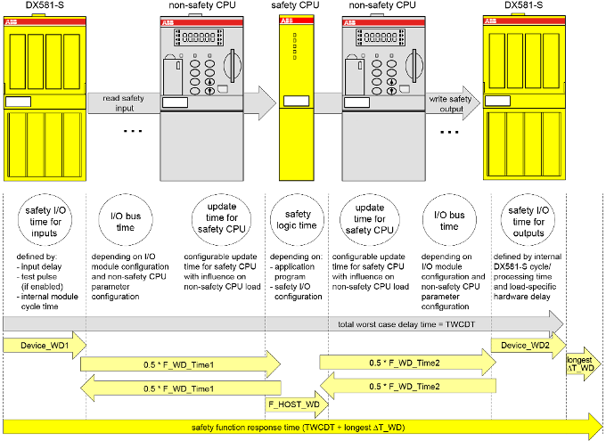
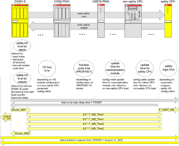
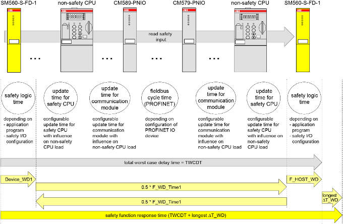
Fig. 529, Fig. 530 and Fig. 531 explain SFRT in more details. The model in Fig. 529 and Fig. 530 includes the stages of input signal reading, safe data transfer, safe logic processing, safe data transfer and safe signal output. The model in Fig. 531 presents safe CPU to CPU communication, which includes the stages of safe logic processing, safe data transfer and safe logic processing.
-
All terms in this figure are further explained ⮫ here.
-
All terms in this figure are further explained ⮫ here.
-
All terms in this figure are further explained ⮫ here.
Explanation of terms related to SFRT
-
Device_WD1 (safety I/O time for inputs) is an internal input device watchdog time in ms which includes:
-
Input delay (variable as parameter; not used for safety analog inputs which have an internal input delay of 67.5 ms in the worst case instead).
-
Input delay accuracy⮫ Table 980 “Input delay accuracy for DI581-S”⮫ Table 982 “Input delay accuracy for DX581-S”.
-
Test pulse low phase (fixed to 1 ms and optional (only if test pulses are used); not used for safety analog inputs).
-
Two times internal cycle time (fixed; AI581-S ➔ 4.5 ms, DX581-S ➔ 5.5 ms and DI581-S ➔ 6.5 ms).
-
-
Device_WD2 (safety I/O time for outputs) is an internal output device watchdog time in ms which includes:
-
Internal safety output device cycle time (fixed; DX581-S ➔ 5.5 ms).
-
Output processing time in DX581-S (fixed to 1.5 ms).
-
Hardware delay (current dependent, e.g., ~1 ms (747 µs at 5 mA) and the maximum of 4 ms under the maximum output current of 500 mA). If more precise values are needed, please contact ABB technical support.
-
-
F_Host_WD (safety logic time) is the time which can be calculated as three times safety application cycle watchdog time. The safety application cycle watchdog time itself is configurable using POU SF_WDOG_TIME_SET. The safety application cycle watchdog time depends on the number of F-Devices, safety application program and system configuration.
-
F_WD_Time1 and F_WD_Time2: The sum represents the data transport time in total via „black channel“. It covers different "black channel" components, like fieldbus cycle time (PROFINET), I/O bus time and update time for safety CPU (configurable as parameter) and communication module.
-
Fieldbus cycle time (PROFINET) depends on the communication settings for the PROFINET IO device where the safety I/O module is attached to. The cycle time is a multiplication of two parameters of the PROFINET IO device.
-
“Send clock”, e.g., for CI501-PNIO and CI502-PNIO: 1 ms, 2 ms or 4 ms
-
“Reduction ratio”, e.g., for CI501-PNIO and CI502-PNIO: 1, 2, 4, 8, 16 ... 512
These values can be selected depending on the defined PROFINET parameters for this PROFINET module.
-
-
The configurable update time for safety CPU and communication modules describes the data transfer time via the communication module bus.
-
With AC500 V2 non-safety CPU:
The update time can be configured within the range of 0 ... 20000 ms for both safety CPU and communication modules.
-
With AC500 V3 non-safety CPU:
The update time for safety CPU can be configured within the range of 1 ... 20000 ms.
The update time for communication modules is configured in the settings of the PROFINET IO controller (CM579-PNIO) and the PROFINET IO device (CM589-PNIO). It is defined by the communication module setting “Bus cycle task”, e.g., in tab “PROFINET-IO-Controller I/O Mapping”. Additional information: ⮫ ““Bus cycle task””
-
-
I/O bus time describes the data transfer time via I/O bus for communication between non-safety CPU and its local I/O bus modules as well as for communication between communication interface modules and their local I/O bus modules.
-
With AC500 V2 non-safety CPU:
The I/O bus cycle time has no fixed pre-defined cycle value. It is defined by the number and type of the configured I/O modules independent from non-safety CPU settings. The I/O bus time contains the following values:
- I/O bus master cycle: 2 ms (2 cycles, 1 ms each)
- I/O bus cycle time: Typically 2 ... 5 ms (2 cycles, 1 ... 2.5 ms each)
In total, the typical range for the I/O bus time is 4 ... 7 ms.
-
With AC500 V3 non-safety CPU:
The I/O bus is driven with a defined cycle time. This I/O bus cycle time relates to I/O bus setting “Bus cycle task” in tab “I/O-Bus I/O Mapping”. Refer to additional information:⮫ ““Bus cycle task””.
A basic definition of I/O bus cycle times is done for non-safety CPU in setting “Bus cycle task” in tab “PLC settings”.
Example for a setting with assignment to a task with 2 ms cycle time (and lower than the defined update time for safety CPU):
- Result for I/O bus master cycle: 2 ms = 2 cycles, 1 ms each
- Result for I/O bus cycle time: Typically 4 ... 5 ms = 2 cycles, 2 ... 2.5 ms each (if the configured task cycle time does not suffice for the I/O bus module assembly, the I/O bus cycle time can be extended to a maximum of 2.5 ms)
In total, the I/O bus time for this example is 6 ... 7 ms.
Refer to additional information:⮫ ““Bus cycle task””, e.g., for I/O bus.
-
With communication interface module CI50x-PNIO:
The I/O bus cycle time has no fixed pre-defined cycle value. It is defined by the number and type of the configured I/O modules independent from communication interface module settings. The I/O bus time contains the following values:
- I/O bus master cycle: 2 ms (2 cycles, 1 ms each)
- I/O bus cycle time: Typically 4 ... 7 ms (2 cycles, 2 ... 3.5 ms each)
In total, the typical range for the I/O bus time is 6 ... 9 ms.
-
Below, a few examples on how to calculate SFRT values under various AC500-S system configurations are presented. In our calculations, we use the following approach, based on⮫ [2] and⮫ [7], which allows us calculating SFRT as:
Equation 2: SFRT = Device_WD1 + 0.5 * F_WD_Time1 + F_Host_WD + 0.5 * F_WD_Time2 + Device_WD2 + Longest ∆T_WD

DANGER
Input delay, input delay accuracy and test pulse low phase are not needed for AI581-S. However, the worst case fixed internal input delay of 67.5 ms shall be used for AI581-S instead.
DANGER
The input delay accuracy has to be calculated based on the following assumptions:
-
It is not used for safety analog inputs.
-
If no test pulses are configured for the given safety digital input, then input delay accuracy can be calculated as 1 % of set input delay value (however, input delay accuracy value must be at least 0.5 ms!).
-
If test pulses are configured for the given safety digital input, then depending on the type of the module (DI581-S or DX581-S) and set input delay value, the following input delay accuracy values can be used in SFRT calculations:⮫ Table 980 “Input delay accuracy for DI581-S”⮫ Table 982 “Input delay accuracy for DX581-S”

NOTICE
⮫ Equation 2 is taken for SFRT calculation with the following reasoning:
-
Device_WD1 and Device_WD2, as worst case delay times for safety I/Os, can be defined as it is shown in Fig. 529 and Fig. 530.
-
To calculate the worst case delay time of "Black channel" components (refer to AC500 non-safety modules in Fig. 529 and Fig. 530), we propose to use half of F_WD_Time1 and F_WD_Time2 instead. F_WD_Time1 and F_WD_Time2 can be empirically obtained for the given AC500 system configuration by tracing the values of tResponseTimeMS for given safety I/Os in the safety application. Use PROFIsafe instance for the given safety I/O ⮫ “SafetyBase_PROFIsafe_LV210_AC500_V22.lib”. F_WD_Time1 and F_WD_Time2 shall be set about 30 % higher than the worst case value observed in the tResponseTimeMS for the given safety I/O.
-
We propose to take F_Host_WD time instead of the worst case delay time of SM560-S safety CPU. F_Host_WD can be calculated as three times the value set using SF_WDOG_TIME_SET POUs. The correct value for SF_WDOG_TIME_SET can be empirically obtained using tracing MAX_TIME output of the same POU in a test run. SF_WDOG_TIME_SET value shall be set about 30 % higher than the worst case value (MAX_TIME) observed in the given safety application to avoid potential availability problems due to triggering of SM560-S safety CPU watchdog.
-
F_WD_Time1 and F_WD_Time2 are the only potential candidates for longest ∆T_WD, because F_Host_WD, Device_WD1 and Device_WD2 are already equal to their worst case delay times. Thus,
Longest ∆T_WD = Max (0.5 * F_WD_Time1; 0.5 * F_WD_Time2)
NOTICE
One could achieve even better SFRT values than those obtained using ⮫ Equation 2 with a more detailed technical analysis. Contact ABB technical support for further details.
NOTICE
You have to set F_WD_Time1 and F_WD_Time2 at least 2 times bigger than the value set using SF_WDOG_TIME_SET time to avoid unintended system stop due to PROFIsafe watchdog expiration.
DANGER
AC500-S safety I/O modules satisfy the requirement of IEC 61131 to bypass a potential undervoltage event with a duration of up to 10 ms. During this undervoltage effect of up to 10 ms, AC500-S safety I/O modules deliver the last valid process value before the undervoltage was detected for safety analog input channels in AI581-S and for safety digital input and output values in DI581-S and DX581-S modules.
If the undervoltage phase is longer than 10 ms then safety I/O module passivation occurs⮫ “Undervoltage / overvoltage”.
If undervoltage events with duration of < 10 ms are frequently observed in the safety application, you have to add 10 ms for AI581-S module in their SFRT calculation to take into account a bypass stage described above. Normally, undervoltage events with duration of < 10 ms are seldom and therefore considered to be low probability faults in the power supply system and can be omitted in the SFRT calculation.
Based on Fig. 529, Fig. 530 and Fig. 531, the following exemplary SFRT values can be achieved for some typical AC500-S configurations using ⮫ Equation 2:
Without PROFINET (DI581-S ➔SM560-S ➔ DX581-S)
SFRT = Device_WD1 + 0.5 * F_WD_Time1 + F_Host_WD + 0.5 * F_WD_Time2 + Device_WD2 + Longest ∆T_WD = 14.5 + 10 + 6 + 10 + 8 + 10 = 58.5 ms
where:
-
Device_WD1 = 1 ms + 0.5 ms + 2 x 6.5 ms = 14.5 ms (no test pulses were used)
-
F_WD_Time1 = 20 ms
-
F_Host_WD = 3 x 2 ms (SF_WDOG_TIME_SET time) = 6 ms
-
F_WD_Time2 = 20 ms
-
Device_WD2 = 8 ms (output current = ~ 5 mA)
-
Longest ∆T_WD = Max (0.5 * F_WD_Time1; 0.5 * F_WD_Time2) = 10 ms
Without PROFINET (DX581-S ➔ SM560-S ➔ DX581-S)
SFRT = Device_WD1 + 0.5 * F_WD_Time1 + F_Host_WD + 0.5 * F_WD_Time2 + Device_WD2 + Longest ∆T_WD = 12.5 + 10 + 6 + 10 + 8 + 10 = 56.5 ms
where:
-
Device_WD1 = 1 ms + 0.5 ms + 2 x 5.5 ms = 12.5 ms (no test pulses were used)
-
F_WD_Time1 = 20 ms
-
F_Host_WD = 3 x 2 ms (SF_WDOG_TIME_SET time) = 6 ms
-
F_WD_Time2 = 20 ms
-
Device_WD2 = 8 ms (output current = ~ 5 mA)
-
Longest ∆T_WD = Max (0.5 * F_WD_Time1; 0.5 * F_WD_Time2) = 10 ms
Without PROFINET (AI581-S ➔ SM560-S ➔ DX581-S)
SFRT = Device_WD1 + 0.5 * F_WD_Time1 + F_Host_WD + 0.5 * F_WD_Time2 + Device_WD2 + Longest ∆T_WD = 76.5 + 10 + 6 + 10 + 8 +10 = 120.5 ms
where:
-
Device_WD1 = 2 x 4.5 ms + 67.5 ms = 76.5 ms
-
F_WD_Time1 = 20 ms
-
F_Host_WD = 3 x 2 ms (SF_WDOG_TIME_SET time) = 6 ms
-
F_WD_Time2 = 20 ms
-
Device_WD2 = 8 ms (output current = ~ 5 mA)
-
Longest ∆T_WD = Max (0.5 * F_WD_Time1; 0.5 * F_WD_Time2) = 10 ms
With PROFINET (DI581-S ➔ SM560-S ➔ DX581-S)
SFRT = Device_WD1 + 0.5 * F_WD_Time1 + F_Host_WD + 0.5 * F_WD_Time2 + Device_WD2 + Longest ∆T_WD = 14.5 + 15 + 6 + 15 + 8 + 15 = 73.5 ms
where:
-
Device_WD1 = 1 ms + 0.5 ms + 2 x 6.5 ms = 14.5 ms (no test pulses were used)
-
F_WD_Time1 = 30 ms
-
F_Host_WD = 3 x 2 ms (SF_WDOG_TIME_SET time) = 6 ms
-
F_WD_Time2 = 30 ms
-
Device_WD2 = 8 ms (output current = ~ 5 mA)
-
Longest ∆T_WD = Max (0.5 * F_WD_Time1; 0.5 * F_WD_Time2) = 15 ms
With PROFINET (DX581-S ➔ SM560-S ➔ DX581-S)
SFRT = Device_WD1 + 0.5 * F_WD_Time1 + F_Host_WD + 0.5 * F_WD_Time2 + Device_WD2 + Longest ∆T_WD = 12.5 + 15 + 6 + 15 + 8 + 15 = 71.5 ms
where:
-
Device_WD1 = 1 ms + 0.5 ms + 2 x 5.5 ms = 12.5 ms (no test pulses were used)
-
F_WD_Time1 = 30 ms
-
F_Host_WD = 3 x 2 ms (SF_WDOG_TIME_SET time) = 6 ms
-
F_WD_Time2 = 30 ms
-
Device_WD2 = 8 ms (output current = ~ 5 mA)
-
Longest ∆T_WD = (Max (0.5 * F_WD_Time1; 0.5 * F_WD_Time2) = 15 ms
With PROFINET (AI581-S ➔ SM560-S ➔ DX581-S)
SFRT = Device_WD1 + 0.5 * F_WD_Time1 + F_Host_WD + 0.5 * F_WD_Time2 + Device_WD2 + Longest ∆T_WD = 76.5 + 15 + 6 + 15 + 8 + 15 = 135.5 ms
where:
-
Device_WD1 = 2 x 4.5 ms + 67.5 ms = 76.5 ms
-
F_WD_Time1 = 30 ms
-
F_Host_WD = 3 x 2 ms (SF_WDOG_TIME_SET time) = 6 ms
-
F_WD_Time2 = 30 ms
-
Device_WD2 = 8 ms (output current = ~ 5 mA)
-
Longest ∆T_WD = Max (0.5 * F_WD_Time1; 0.5 * F_WD_Time2) = 15 ms
With PROFINET (SM560-S-FD-1 ➔ SM560-S)
SFRT = Device_WD1 + 0.5 * F_WD_Time1 + F_Host_WD + Longest ∆T_WD = 9 + 25 + 6 + 25 = 65 ms
where:
-
Device_WD1 = 3 x 3 ms (SF_WDOG_TIME_SET time) = 9 ms
-
F_WD_Time1 = 50 ms
-
F_Host_WD = 3 x 2 ms (SF_WDOG_TIME_SET time) = 6 ms
-
Longest ∆T_WD = 0.5 * F_WD_Time1 = 25 ms
NOTICE
SFRT calculation for such cases as SM560-S-FD-4 ➔ SM560-S, SM560-S ➔ SM560-S-FD-1, SM560-S ➔ SM560-S-FD-4, etc. can be calculated in a similar way as it is shown in Fig. 531.
DANGER
Mistakes in SFRT calculation can lead to death or severe personal injury, especially in such applications like presses, robotic cells, etc.
NOTICE
The high priority tasks on non-safety CPU, which are a part of the "black channel" for safety communication, may affect TWCDT for AC500-S safety PLC.